Industries · Semiconductor (High Purity)
Semiconductor & High-Purity Analytical Applications
Define the Materials, Connections, and Handling Requirements Up Front
Semiconductor and high-purity applications place particular emphasis on contamination control and the suitability of every wetted component. AES can review requirements for analytical and supporting assemblies involving process gases, chemicals, water, and critical utilities.
Assemblies
Sample handling
Fabrication
Panels, racks, cabinets
Interfaces
Field and documentation
Specification
Scope development
Requirements
High-Purity Analytical Requirements
A high-purity application may be sensitive to particles, moisture, trace contaminants, or material interactions that would be less significant in another industrial service.
A high-purity application may be sensitive to:
Project Areas
Project Areas to Discuss With AES
Three areas to define up front for a high-purity project.
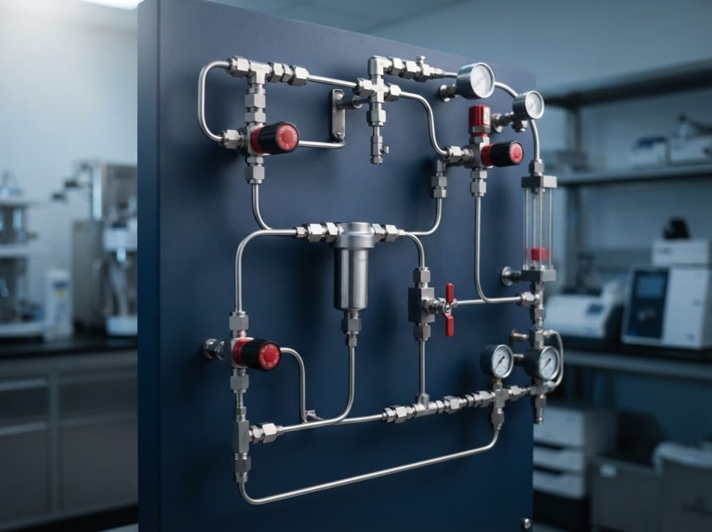
Analytical and Sample Handling Assemblies
Review the specified analyzer, sample-path components, materials, and connection requirements. The scope should identify how the assembly will be protected from contamination during fabrication, delivery, and installation.

Custom Panels, Racks, and Cabinets
Define supports and housings around equipment dimensions, access, utility connections, and the facility's construction requirements. Structural fabrication and wetted-system fabrication may have different quality and handling needs.
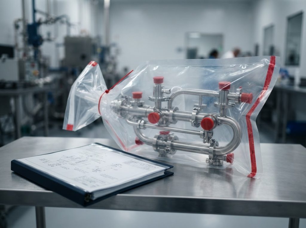
Field Interfaces and Documentation
Establish the installation boundary, approved joining methods, test requirements, and turnover records before mobilization. Site-specific work protocols and specialist qualifications must be confirmed for the proposed assignment.
Specification-Led
Specification-Led Scope Development
Provide the required purity limits, materials, surface finish, leak criteria, cleaning and packaging requirements, and applicable facility standards. If cleanroom fabrication, orbital welding, passivation, or a specific certification is required, identify it for explicit capability and qualification review; none is implied by this page.
Andon, AES's parent company, publicly includes high-purity products and semiconductor applications within its broader offering. That relationship provides corporate context, while the party responsible for each proposed service must still be confirmed.
Discuss a High-Purity Application →Provide:
Why AES
Why Start With AES?
A clearly defined assembly and interface scope helps the project team distinguish the equipment it needs from the fabrication and field qualifications required to deliver it. AES can review the proposed work and identify requirements that need additional technical confirmation before commitment.
Equipment
Fabrication qualifications
Field qualifications
Does this page imply cleanroom-certified fabrication?
No. Cleanroom conditions, cleanliness verification, personnel qualifications, and certification requirements must be explicitly confirmed for the specific scope.
Can customer-specified components be used?
Yes, as the basis for project review. Provide the approved component list, traceability requirements, and any restrictions on substitutions or handling.
Can AES support both gas and liquid applications?
Each application must be reviewed separately. Materials, contamination concerns, joining methods, and testing can differ significantly between high-purity gases, chemicals, and water systems.
Discuss Your High-Purity Assembly Requirements
Send AES the approved specifications and proposed work scope to establish the equipment, fabrication, and qualification requirements for review.
Discuss a High-Purity Application →